| Forming the Pattern on the wafer |
After the light exposure on the photomask, the pattern is printed and developed on the wafer. |
 |
| Etching |
Etching the oxidation layer on the wafer partially, you make I.C |
 |
| I.C. Completion |
After about 300-400 process, finally I.C. can be completed on the wafer. |
| Back Grind |
Laminating the Tape for protecting the surface of wafer
Before grinding the wafer face, laminate the protective tape to prevent foreign material from penetrating. |
 |
Grinding the Wafer Surface
To thin the wafer, it grinds the back side of the wafer by suitable thickness |
 |
Removing the protective tape
You remove the protective tape laminated to protect the surface.
* In case of UV tape, remove it after UV irradiation. |
 |
| Dicing |
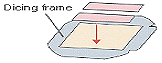
Laminating the Tape
In dicing the wafer, the tape is laminated on the frame and wafer to prevent chips from flying. |
 |
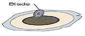
Dicing
The wafer is diced for suitable chip size. |
 |
Pick up
The sawn-chip on the wafer is picked up.
* In case of UV tape, after UV irradiation the chip is picked up. |
|
Being Package
|
After die bonding, the chip is to be package. |
|
Package Dicing
|
Tape Laminate
In package dicing, the tape is laminated on the dicing frame and package to prevent chips from flying. |
 |
Dicing
Each package is sawn for suitable size. |
 |
Pick up
The sawn package is picked up.
* In case of UV tape, the package is picked up after UV irradiation.
|
|
Completion the IC package
|
After inspection and reliability test, the package is completed. |